• P-ISSN 0974-6846 E-ISSN 0974-5645

Indian Journal of Science and Technology

Article

Indian Journal of Science and Technology

Year: 2020, Volume: 13, Issue: 29, Pages: 2973-2980

Original Article

Structural analysis of the chemical vapour deposition grown molybdenum disulphide nanofilms for multifaceted applications

Received Date:25 July 2020, Accepted Date:30 July 2020, Published Date:11 August 2020

Abstract

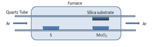
Background/Objectives: In recent years, the research on molybdenum disulphide (MoS2) has gained significance because of its unique properties and ease of incorporation in hybrid structures, which makes it one of the most suitable materials for devices and multifaceted Applications. The objective of the study is to synthesize MoS2 nanofilms and then to characterize them through X-ray diffraction (XRD) technique. Methods: In this study, MoS2 nanofilms are synthesized on silicon dioxide substrates by the thermal Chemical Vapour Deposition (CVD) technique, where molybdenum trioxide (MoO3) (VI) powder and sulphur (S) flakes are used as precursors. Findings:X-ray diffraction (XRD) measurements have been carried out for the thermal CVD grown MoS2 nanofilm samples. Further, the observed XRD data has been analyzed and the structural analysis of synthesized MoS2 nanofilms is presented in this report. Furthermore, the experimentally observed findings are compared with the standard findings and shown that they are resembling closely. Novelty/Applications: In order to highlight the scope of our work, the important applications, of the molybdenum disulphide nanostructures are also discussed, that make MoS2 nanostructures attractive candidates in fields as diverse as energy, environmental, biomedical and semiconductors.

Keywords: Chemical vapour deposition; molybdenum disulphide; nanofilms;XRD; transition metal dichalcogenide

References

  1. Mak KF, Lee C, Hone J, Shan J, Heinz TF. Atomically ThinMoS2: A New Direct-Gap Semiconductor. Physical Review Letters. 2010;105(13):136805. Available from: https://dx.doi.org/10.1103/physrevlett.105.136805
  2. Zhang X, Zhang S, Xie Y, Huang J, Wang L, Cui Y, et al. Tailoring the nonlinear optical performance of two-dimensional MoS2 nanofilms via defect engineering. Nanoscale. 2018;10(37):17924–17932. Available from: https://doi.org/10.1039/C8NR05653F
  3. Stern C, Grinvald S, Kirshner M, Sinai O, Oksman M, Alon H, et al. Growth Mechanisms and Electronic Properties of Vertically Aligned MoS2. Scientific Reports. 2018;8(1):16480. Available from: https://dx.doi.org/10.1038/s41598-018-34222-z
  4. Son D, Chae S, Kim M, Choi MK, Yang J, Park K, et al. Colloidal synthesis of uniform-sized molybdenum disulfide nanosheets for wafer-scale flexible nonvolatile memory. Advanced Materials. 2016;28. Available from: https://doi.org/10.1002/adma.201602391
  5. Shinde SM, Kalita G, Tanemura M. Fabrication of poly(methyl methacrylate)-MoS2/graphene heterostructure for memory device application. Journal of Applied Physics. 2014;116(21):214306. Available from: https://dx.doi.org/10.1063/1.4903552
  6. Wang Z, Mi B. Environmental applications of 2D molybdenum disulfide (MoS2) nanosheets. Environmental Science & Technology. 2017;51(15):8229–8244. Available from: https://doi.org/10.1021/acs.est.7b01466
  7. Liu T, Liu Z. 2D MoS2 nanostructures for biomedical applications. Advanced Healthcare Materials. 2018;7(8):1701158. Available from: https://doi.org/10.1002/adhm.201701158
  8. Lopez-Sanchez O, Lembke D, Kayci M, Radenovic A, Kis A. Ultrasensitive photodetectors based on monolayer MoS2. Nature Nanotechnology. 2013;8(7):497–501. Available from: https://dx.doi.org/10.1038/nnano.2013.100
  9. Pu J, Yomogida Y, Liu KK, Li LJ, Iwasa Y, Takenobu T. Highly Flexible MoS2 Thin-Film Transistors with Ion Gel Dielectrics. Nano Letters. 2012;12(8):4013–4017. Available from: https://dx.doi.org/10.1021/nl301335q
  10. Zhang Y, Tan YW, Stormer HL, Kim P. Experimental observation of the quantum Hall effect and Berry's phase in graphene. Nature. 2005;438(7065):201–204. Available from: https://dx.doi.org/10.1038/nature04235
  11. Balandin AA, Ghosh S, Bao W, Calizo I, Teweldebrhan D, Miao F, et al. Superior Thermal Conductivity of Single-Layer Graphene. Nano Letters. 2008;8(3):902–907. Available from: https://dx.doi.org/10.1021/nl0731872
  12. Bolotin KI, Sikes KJ, Jiang Z, Klima M, Fudenberg G, Hone J, et al. Ultrahigh electron mobility in suspended graphene. Solid State Communications. 2008;146(9-10):351–355. Available from: https://dx.doi.org/10.1016/j.ssc.2008.02.024
  13. Lee C, Wei X, Kysar JW, Hone J. Measurement of the Elastic Properties and Intrinsic Strength of Monolayer Graphene. Science. 2008;321(5887):385–388. Available from: https://dx.doi.org/10.1126/science.1157996
  14. Sun Z, Dong N, Xie K, Xia W, König D, Nagaiah TC, et al. Nanostructured Few-Layer Graphene with Superior Optical Limiting Properties Fabricated by a Catalytic Steam Etching Process. The Journal of Physical Chemistry C. 2013;117(22):11811–11817. Available from: https://dx.doi.org/10.1021/jp401736n
  15. Kim K, Lara-Avila S, He H, Kang H, Park Y, Yakimova R, et al. Thermal Stability of Epitaxial Graphene Electrodes for Conductive Polymer Nanofiber Devices. Crystals. 2017;7(12):378. Available from: https://dx.doi.org/10.3390/cryst7120378
  16. Geim AK, Novoselov KS. The rise of graphene. Nature Materials. 2007;6(3):183–191. Available from: https://dx.doi.org/10.1038/nmat1849
  17. Reina G, González-Domínguez JM, Criado A, Vázquez E, Bianco A, Prato M. Promises, facts and challenges for graphene in biomedical applications. Chemical Society Reviews. 2017;46(15):4400–4416. Available from: https://dx.doi.org/10.1039/c7cs00363c
  18. Kuhn KJ. Considerations for Ultimate CMOS Scaling. IEEE Transactions on Electron Devices. 2012;59(7):1813–1828. Available from: https://dx.doi.org/10.1109/ted.2012.2193129
  19. Schwierz F. Graphene transistors. Nature Nanotechnology. 2010;5(7):487–496. Available from: https://dx.doi.org/10.1038/nnano.2010.89
  20. Schwierz F. Graphene Transistors: Status, Prospects, and Problems. Proceedings of the IEEE. 2013;101(7):1567–1584. Available from: https://dx.doi.org/10.1109/jproc.2013.2257633
  21. Sun J, Li X, Guo W, Zhao M, Fan X, Dong Y, et al. Synthesis methods of two-dimensional MoS2: a brief review. Crystals. 2017;7(7). Available from: https://doi.org/10.3390/cryst7070198
  22. Deokar G, Vignaud D, Arenal R, Louette P, Colomer JF. Synthesis and characterization of MoS2nanosheets. Nanotechnology. 2016;27(7):075604. Available from: https://dx.doi.org/10.1088/0957-4484/27/7/075604
  23. Liu KK, Zhang W, Lee YH, Lin YC, Chang MT, Su CY, et al. Growth of large-area and highly crystalline MoS2 thin layers on insulating substrates. Nano Letters. 2012;12(3):1538–1582. Available from: https://doi.org/10.1021/nl2043612
  24. Wang H, Skeldon P, Thompson G, Wood GC. Synthesis and characterization of molybdenum disulphide formed from ammonium tetrathiomolybdate. Journal of Materials Science. 1997;32:497–502. Available from: https://doi.org/10.1023/a:1018538424373
  25. Liu N, Kim P, Kim JH, Ye JH, Kim S, Lee CJ. Large-area atomically thin MoS2 nanosheets prepared using electrochemical exfoliation. ACS Nano. 2014;8(7):6902–6910. Available from: https://doi.org/10.1021/nn5016242
  26. Magda GZ, Pető J, Dobrik G, Hwang C, Biró LP, Tapasztó L. Exfoliation of large-area transition metal chalcogenide single layers. Scientific Reports. 2015;5(1):14714. Available from: https://dx.doi.org/10.1038/srep14714
  27. Chen M, Nam H, Wi S, Priessnitz G, Gunawan IM, Liang X. Multibit Data Storage States Formed in Plasma-Treated MoS2 Transistors. ACS Nano. 2014;8(4):4023–4032. Available from: https://dx.doi.org/10.1021/nn501181t
  28. Zhang E, Wang W, Zhang C, Jin Y, Zhu G, Sun Q, et al. Tunable charge-trap memory based on few-layer MoS2. ACS Nano. 2015;9(1):612–619. Available from: https://doi.org/10.1021/nn5059419
  29. Yin Z, Zeng Z, Liu J, He Q, Chen P, Zhang H. Memory devices using a mixture of MoS2 and graphene oxide as the active layer. Small. 2013;9(5):727–731. Available from: https://doi.org/10.1002/smll.201201940
  30. Cao X, Shi Y, Shi W, Rui X, Yan Q, Kong J, et al. Preparation of MoS 2-coated three-dimensional graphene networks for high-performance anode material in lithium-ion batteries. Small. 2013;9(20):3433–3438. Available from: https://doi.org/10.1002/smll.201202697
  31. Tang K, Wang L, Geng H, Qiu J, Cao H, Liu X. Molybdenum disulfide (MoS2) nanosheets vertically coated on titanium for disinfection in the dark”. Arabian Journal of Chemistry. 13(1):1612–1623. Available from: https://doi.org/10.1016/j.arabjc.2017.12.013
  32. Bazaka K, Levchenko I, Lim JWM, Baranov O, Corbella C, Xu S, et al. MoS2-based nanostructures: synthesis and applications in medicine. Journal of Physics D: Applied Physics. 2019;52(18):183001. Available from: https://dx.doi.org/10.1088/1361-6463/ab03b3
  33. Sobanska Z, Zapor L, Szparaga M, Stepnik M. Biological effects of molybdenum compounds in nanosized forms under in vitro and in vivo conditions. International Journal of Occupational Medicine and Environmental Health. 2020;33(1):1–19. Available from: https://dx.doi.org/10.13075/ijomeh.1896.01411
  34. Romanov RI, Kozodaev MG, Myakota DI, Chernikova AG, Novikov SM, Volkov VS, et al. Synthesis of Large Area Two-Dimensional MoS2 Films by Sulfurization of Atomic Layer Deposited MoO3 Thin Film for Nanoelectronic Applications. ACS Applied Nano Materials. 2019;2(12):7521–7531. Available from: https://dx.doi.org/10.1021/acsanm.9b01539
  35. Ullah MS, Yousuf AHB, Es-Sakhi AD, Chowdhury MH. Analysis of optical and electronic properties of MoS2 for optoelectronics and FET applications. AIP Conference Proceedings. 2018;1957(1). Available from: https://doi.org/10.1063/1.5034320
  36. Xia Y, Hu C, Guo S, Zhang L, Wang M, Peng J, et al. Sulfur-Vacancy-Enriched MoS2 Nanosheets Based Heterostructures for Near-Infrared Optoelectronic NO2 Sensing. ACS Applied Nano Materials. 2020;3(1):665–673. Available from: https://dx.doi.org/10.1021/acsanm.9b02180
  37. Zhang D, Jiang C, Wu J. Layer-by-layer assembled In2O3 nanocubes/flower-like MoS2 nanofilm for room temperature formaldehyde sensing. Sensors and Actuators B: Chemical. 2018;273:176–184. Available from: https://doi.org/10.1016/j.snb.2018.06.044

Copyright

© 2020 Saini et al.This is an open-access article distributed under the terms of the Creative Commons Attribution License, which permits unrestricted use, distribution, and reproduction in any medium, provided the original author and source are credited. Published By Indian Society for Education and Environment (iSee).

DON'T MISS OUT!

Subscribe now for latest articles and news.