Indian Journal of Science and Technology
Year: 2021, Volume: 14, Issue: 1, Pages: 33-45
Original Article
Vidhi Raval1*, Amit Patel2
1PhD Scholar, Charusat University, CSPIT, Changa, Anand, 388421, Gujarat, India. Tel.: +091745255229
2Assistant Professor, Charusat University, CSPIT, Changa, Anand, 388421, Gujarat, India
*Corresponding Author
Tel: +091-745255229
Email: [email protected]
Received Date:15 October 2020, Accepted Date:12 December 2020, Published Date:11 January 2021
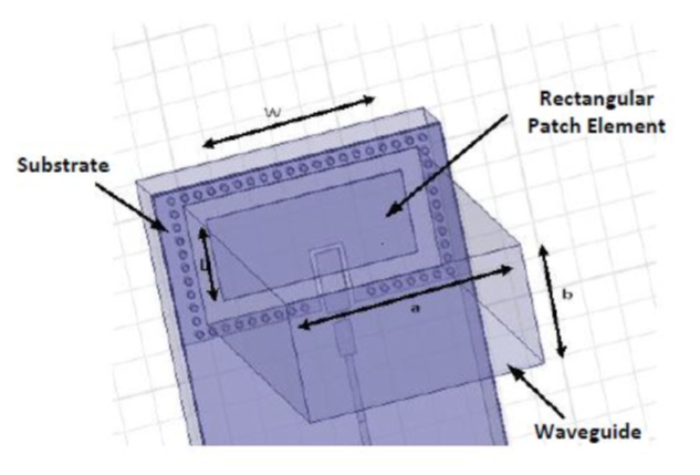
Background/Objectives: To design, analyze and fabricate aperture coupled waveguide to microstrip transition for Ka-Band where energy is coupled through slot in ground plane and a metal patch placed over the substrate. Methods: Impedance matching approach has been adopted for transition design. Microstrip line is inserted into the waveguide through aperture acting as a probe. Followed by inductive line and transformer line for impedance translation between waveguide and microstrip line. Waveguide transition has been designed using Ansoft High Frequency Structure Simulator (HFSS) full-wave EM simulator. Findings: Designed transition shows return loss performance better than 15 dB and insertion loss better than 0.5 dB for back to back configuration over a frequency band of 34 – 36 GHz. Transition is fabricated on RT5580 Duroid substrate (2r= 2:2) with substrate thickness 0.254 mm. Measured results show return loss better than 25 dB and insertion loss less than 1 dB over a frequency band of 34-36 GHz. Table 2 shows comparison of present design with previously reported designs in terms of performance. Novelty/Applications: Comparison of the presented transition shows superior performance to previously reported transition designs in terms of transition bandwidth and insertion loss. Aperture coupled transitions can be widely used for space applications where hermetic sealing is required and it saves extra effort for sealing. Certain RF circuit applications require narrowband waveguide transitions to attain required performance, in this case aperture coupled transition can be a good option and its integration with RF circuits is also easy. Fabricated transition design results show good agreement with simulated results so it can be concluded that design is tolerant to fabrication errors. Transition has been fabricated using standard PCB process so production of such transition can be done easily without requirement of any special facility for fabrication.
Keywords: Aperture coupled transition; waveguide; microstrip; kaBand;hermetically sealed
© 2021 Raval & Patel.This is an open access article distributed under the terms of the Creative Commons Attribution License, which permits unrestricted use, distribution, and reproduction in any medium, provided the original author and source are credited. Published By Indian Society for Education and Environment (iSee)
Subscribe now for latest articles and news.