Indian Journal of Science and Technology
Year: 2021, Volume: 14, Issue: 9, Pages: 776-786
Original Article
B S Premananda1*, Archit Bajpai1, G Shakthivel1, A R Anurag1
1Department of Electronics and Telecommunication, RV College of Engineering, Bengaluru,
560059, India
*Corresponding Author
Email: [email protected]
Received Date:24 February 2021, Accepted Date:09 March 2021, Published Date:19 March 2021
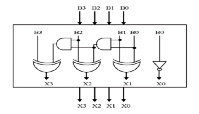
Background: An adder is the basic building block of any circuitry. Most ripple carry adders suffer from carry rippling which constrains its performance due to increased delay though they occupy less area. Objectives: To design and implement a high speed adder to overcome the carry rippling, which should consume less power and also operate at higher frequency. Method: Squareroot CSLA architecture is designed by replacing ripple carry adder with of Add- One Circuit (AOC) to minimize the area and carry rippling delay. Improved Pass-Gate Adiabatic Logic (IPGL) is incorporated in the proposed SCLSA to reduce power and to increase frequency of operation. Cadence Virtuoso and Spectre is used to design and simulate the adder circuits in CMOS 180nm technology. Findings: We proposed SCSLA adder, which consumed 89% lesser power compared to the reference architecture at 400 MHz operating frequency with a power saving factor of 7.3. Results were verified by simulating up to 1 GHz frequency. Novelty: Incorporation of AOC in the design of square-root CSLA with adiabatic logic (IPGL) incorporated results in lesser power consumption and also adder operates in the higher frequency (GHz).
Keywords: AL; AOC; BEC; IPGL; low power
© 2021 Premananda et al.This is an open access article distributed under the terms of the Creative Commons Attribution License, which permits unrestricted use, distribution, and reproduction in any medium, provided the original author and source are credited. Published By Indian Society for Education and Environment (iSee)
Subscribe now for latest articles and news.